- Pre-Layout Analysis
-
Pre-Layout Design Flow 0 hr 2 min
-
Transmission Line Libraries 0 hr 2 min
-
Controlled Impedance Line Designer 0 hr 14 min
-
Via Designer 0 hr 18 min
-
Build Channel Models 0 hr 2 min
-
SnP Component 0 hr 4 min
-
Lab 1A: Controlled Impedance Line Designer 1 hr 30 min
-
Lab 1B: Via Designer 1 hr 30 min
-
Knowledge Check 0 hr 5 min
- Channel Simulation
-
Channel Simulator Modes 0 hr 8 min
-
IBIS-AMI Models 0 hr 12 min
-
Channel Simulation Palette 0 hr 8 min
-
Channel Simulation Results 0 hr 10 min
-
Memory Designer 0 hr 14 min
-
Chiplets 0 hr 4 min
-
Lab 2A: Compare Backdrilled to Not Backdrilled Vias 1 hr 30 min
-
Lab 2B: Optimize the Channel Performance 1 hr 0 min
-
Lab 2C: Channel Simulation with IBIS-AMI Model 1 hr 0 min
-
Lab 3: Mix and Match Simulation 1 hr 0 min
-
Lab 4: PAM4 Signal Channel Simulation 1 hr 0 min
-
Knowledge Check 0 hr 5 min
- Summary and Next Step
-
Claim your certificate
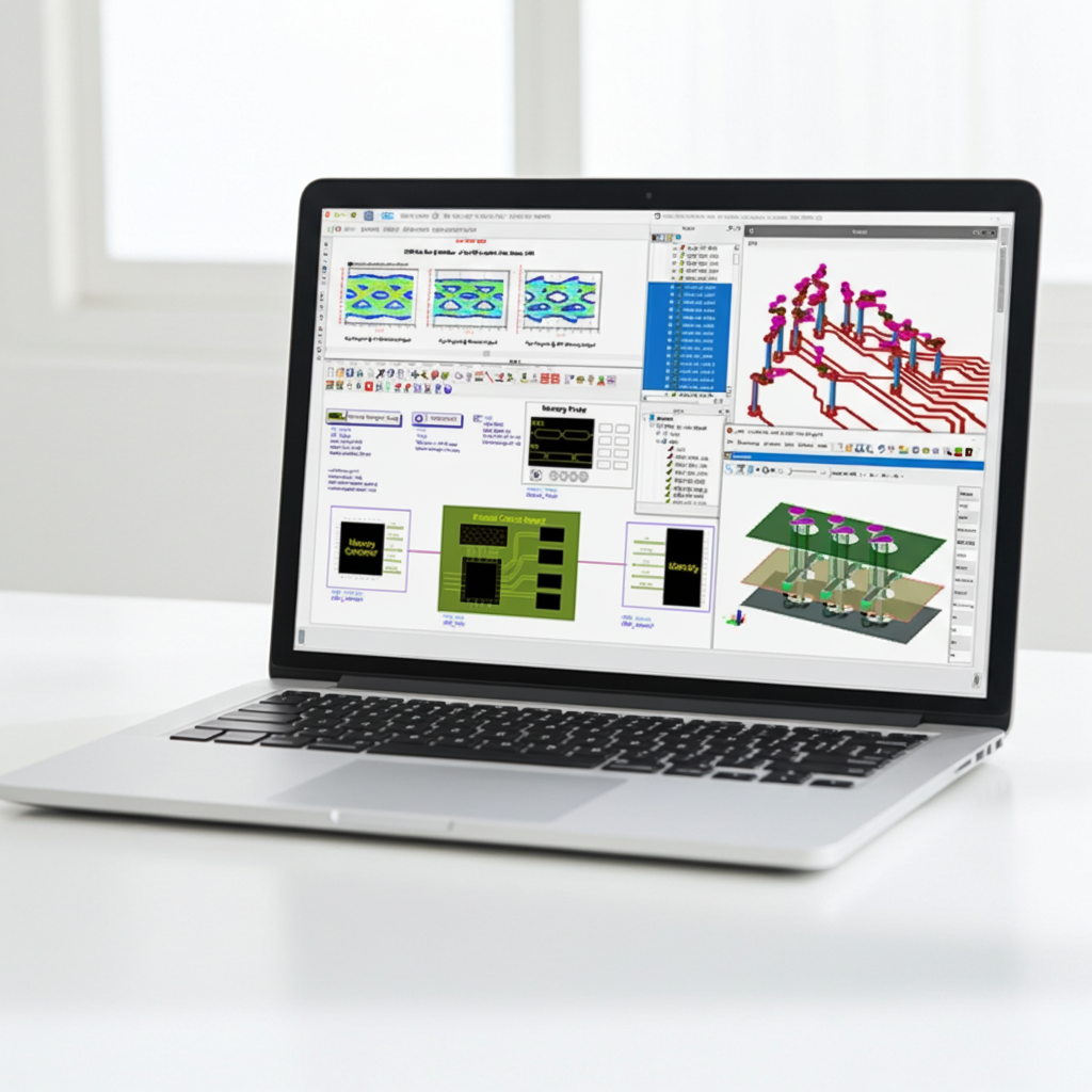
Pre-Layout Analysis and Channel Simulation
You will master the pre-layout phase by optimizing substrate stacking, trace width/spacing, and via architecture for signal integrity.
+ Learning Objectives
Pre-Layout Analysis
- Controlled Impedance Line Designer, Via Designer, Transmission Line Libraries
- Lab 1: Design a differential pair on different layer with CILD & design differential vias with via designer tool.
Channel Simulation
- Channel Simulation using IBIS-AMI Model, Mix and Match Simulations, NRZ and PAM-X Signal
- Lab 2: Build a channel, channel simulation of backdrilled vias, comparison of backdrilled vias with non backdrilled vias (through vias), optimize the channel performance, channel simulation with IBIS-AMI model, mix and match simulation, PAM4 signal channel simulation.
+ Content Types
- Video Lessons
- Hands-on Labs
- Knowledge Check
+ Who should take this course?
- For SI/PI/HSD engineers
+ Prerequisites