Lab: S-Parameter Analysis
This lab covers schematic creation, parameterization, tuning, and data display. You will build a transmission line using lumped elements, transition it to a distributed model, and analyze its group delay.
FREE
1 hr 30 min
auto-registration
Hands on lab
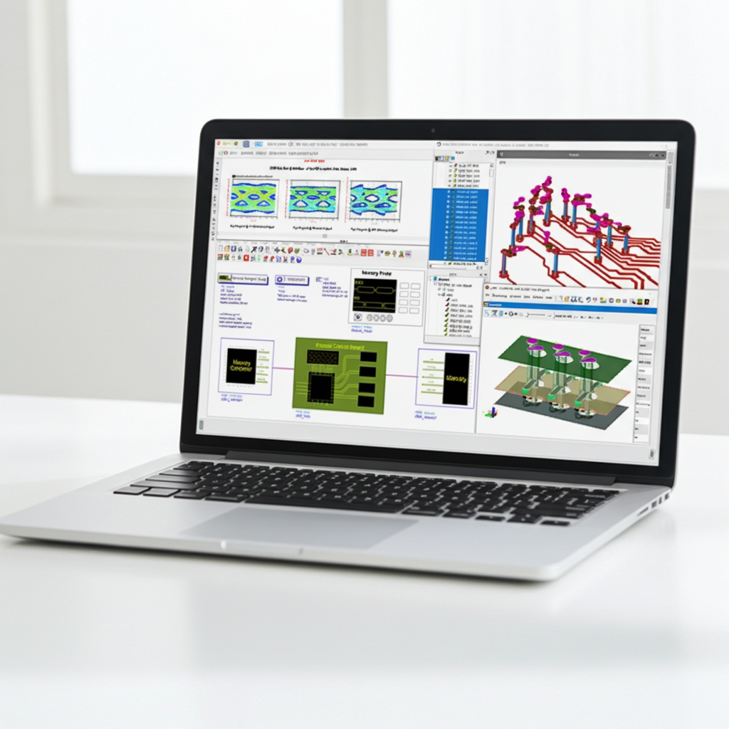
Lab: Working with ODB++ Layouts
In this lab, you will learn to manage imported PCB layouts. Tasks include importing an ODB++ layout with its associated technology file, investigating the layout architecture, and utilizing the Net-based connectivity mode to check layout interconnects
FREE
1 hr 30 min
auto-registration
Hands on lab
Lab: Learn SIPro/PIPro Flow
Master the SIPro/PIPro interface, visibility controls, analysis setup, net/component filtering, and port creation to extract interconnect S-parameters from complex PCBs.
FREE
2 hr 0 min
auto-registration
Hands on lab
Lab: Power-Aware Signal Integrity Analysis
Set up the power-aware SI analysis for PCB: define ports for the DQ5 line and power nets, assign component models, execute the simulation, and generate the final subcircuit.
FREE
1 hr 45 min
auto-registration
Hands on lab
Lab: Comparing Ideal and Power-Aware Channel Interconnects
Evaluate the eye diagram under two conditions: first, with ideal VRM, FPGA, and memory IC connections; second, using a power-aware channel model to capture power plane impedance, data line SI, and coupling effects (SSN/ground bounce).
FREE
0 hr 45 min
auto-registration
Hands on lab
Lab: VRM to IC Voltage Drop Analysis
In this lab, you will analyze the voltage drop from the VRM to the memory ICs to ensure the DC voltage at the chip input is sufficiently large for stable operation. You will run a PIPro DC analysis, inspect the results, and generate a test bench and subcircuit.
FREE
1 hr 0 min
auto-registration
Hands on lab
Lab: PDN AC Impedance Analysis
Convert a DC IR drop analysis into a PIPro AC PDN impedance analysis, map component models to analyze chip-to-VRM impedance profiles with decaps, and perform decap optimization.
FREE
1 hr 30 min
auto-registration
Hands on lab